


Chips for Europe Initiative
- Home
- Chips for Europe Initiative
Europe stands at a pivotal moment in its technological trajectory. As global competition intensifies and demand for advanced digital infrastructure accelerates, the EU faces a growing innovation gap that threatens its economic resilience and strategic autonomy.
Semiconductor technologies, which are fundamental to digitalisation, secure communications, industrial competitiveness, and energy‑efficient systems, have become a decisive factor in global competitiveness. Yet Europe remains heavily dependent on external suppliers and geographically concentrated production chains, exposing its industries to significant supply risks and geopolitical vulnerabilities.
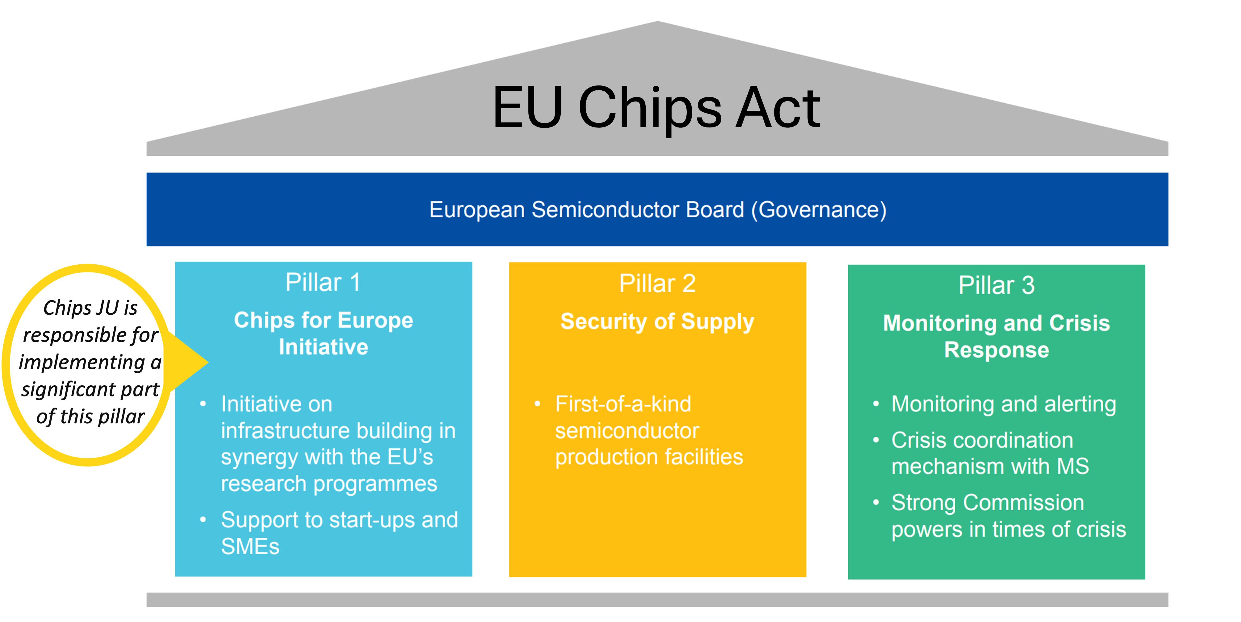
The Chips Act, adopted in 2023, is the Union’s strategic response to this challenge. It represents a comprehensive effort to reinforce Europe’s position in the global semiconductor landscape by expanding design and manufacturing capabilities, strengthening research and development, and supporting the emergence of a robust, interconnected ecosystem.
By addressing structural weaknesses, such as limited production capacity at leading‑edge nodes, shortages of skilled talent, and barriers faced by SMEs, the Chips Act aims to secure Europe’s long‑term technological sovereignty.
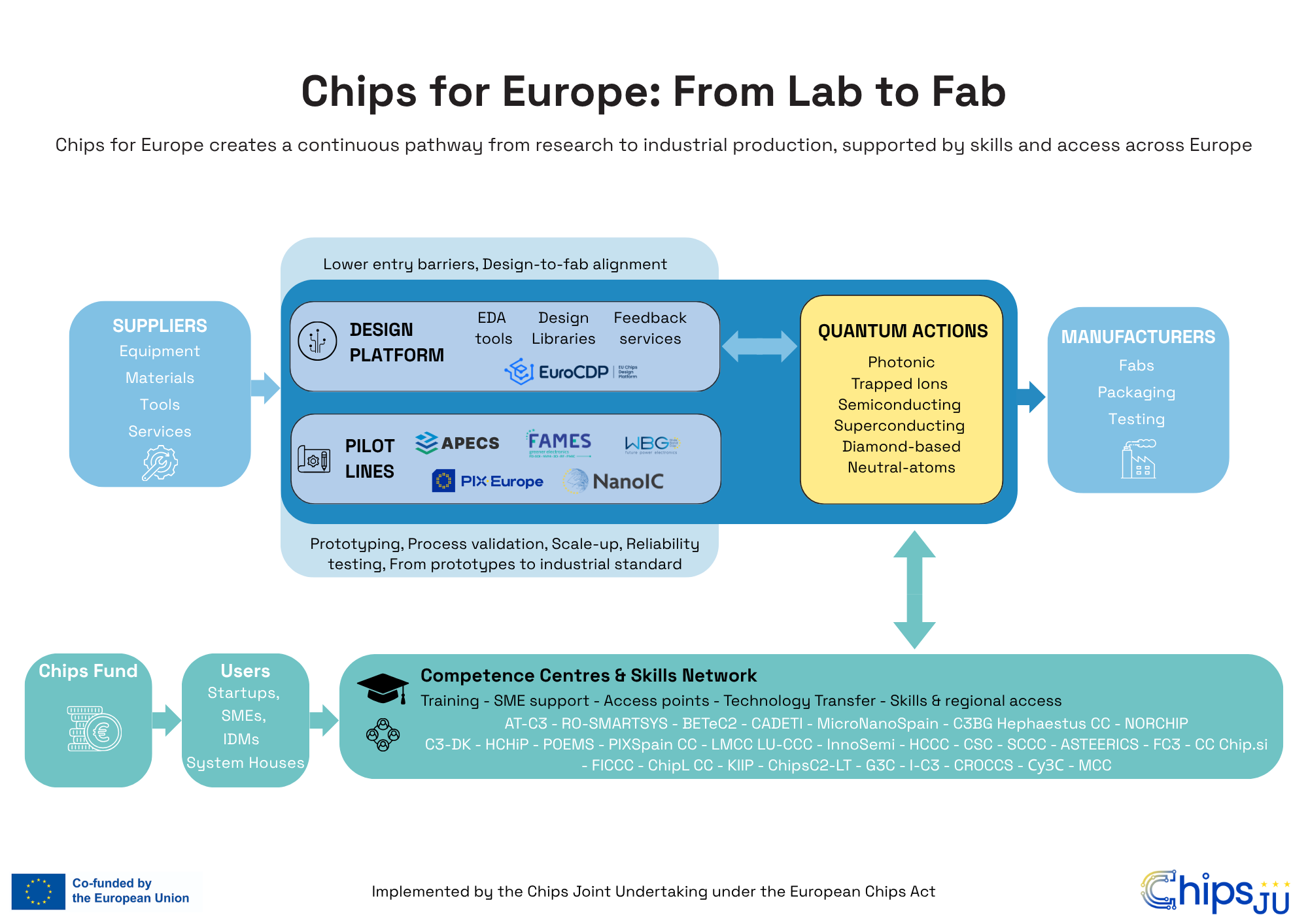
The Chips for Europe Initiative is the first pillar of the Chips Act, designed to reinforce the Union’s competitiveness, resilience, and innovation capacity in semiconductor technologies. Under the Chips JU, the Initiative focuses on five core operational areas to strengthen the Union’s semiconductor ecosystem.
Advanced Pilot Lines
To bridge the gap between the laboratory to commercial production, the Initiative supports a network of advanced Pilot Lines. These facilities provide the necessary infrastructure for producing, testing, and validating breakthrough technologies in an open and accessible way. Key focus areas include fully depleted silicon on insulator down to 10-7 nm, advanced gate-all-around and leading-edge nodes (e.g. below 2 nm), complemented by Pilot Lines for 3D heterogeneous systems integration, advanced packaging and integrated photonics.
Design Platform
The Initiative establishes a Union-wide virtual Design Platform to reinforce Europe’s design capacity. This cloud-based environment integrates a wide range of design facilities—from IP libraries to Electronic Design Automation (EDA) tools—and support services. By connecting the communities of design houses, start-ups, SMEs, and research organisations, the platform stimulates cooperation and provides virtual prototype solutions based on the co-development of technology. New IP blocks and new system concepts can be tested and validated on the Pilot Lines through early process design kits, providing immediate feedback to refine and improve the models before transferring to manufacturing.
Competence Centres
To ensure that the benefits of the Chips Act reach across the entire Union, a network of Competence Centres has been established. These centres provide technical expertise and experimentation facilities to stakeholders, particularly SMEs and start-ups. They support access to the Design Platform and Pilot Lines, offering specialised services and support to help companies improve their design capabilities and integrate advanced semiconductor technologies into their products.
Quantum Actions
The Initiative also addresses the specific needs of the future generation of information processing components by building capacities for the development of quantum chips. This includes supporting the development of design libraries for quantum chips, dedicated pilots, and facilities for testing and validating advanced quantum components. These actions aim to accelerate the transition of quantum technologies from research to industrial application, securing Europe's leadership in this emerging field. Targeted quantum technologies range from superconducting circuits to photonics, silicon/germanium quantum dots, diamond materials, neutral atom chips, and ion‑trap architectures.
Skills Development
To address the shortage of skilled professionals, the Initiative promotes education, training, and reskilling. It supports the development of a highly qualified workforce through access to postgraduate programs, short-term training courses, and job placements in advanced laboratories. By fostering a talent pool of designers and engineers, the Initiative ensures that the European semiconductor industry has the human capital necessary to sustain long-term innovation and production.


